| Models | H5CX-A[]-N | H5CX-A11[]-N | H5CX-L8[]-N | |
|---|---|---|---|---|
| Classification | Standard Type | Economy Type | ||
| Ratings | Power supply
voltage *1 |
100 to 240 VAC 50/60 Hz
12 to 24 VDC/24 VAC 50/60 Hz |
||
| Operating voltage
fluctuation range |
85% to 110% of rated supply voltage (90% to 110% at 12 to 24 VDC) | |||
| Power consumption | Approx. 6.2 VA at 100 to 240 VAC, Approx. 5.1 VA/2.4 W at 24 VAC/12 to 24 VDC *2 | |||
| Mounting method | Flush mounting | Flush mounting, surface mounting, DIN track mounting | ||
| External connections | Screw terminals | 11-pin socket | 8-pin socket | |
| Degree of protection | IEC IP66, UL508 Type 4X (indoors) for panel surface only and when Y92S-29
Waterproof Packing is used |
|||
| Digits | 4 digits | |||
| Time ranges | 0.001 s to 9.999 s, 0.01 s to 99.99 s, 0.1 s to 999.9 s, 1 s to 9999 s, 1 s ti 99 min 59 s
0.1 m to 999.9 min, 1 min to 9999 min, 1 min to 99 h 59 min, 0.1 h to 999.9 h, 1 h to 9999 h |
|||
| Timer mode | Elapsed time (Up), remaining time (Down) (selectable) | |||
| Inputs | Input signals | Signal, Reset, Gate | Signal, Reset
(no inputs on models with instantaneous contact outputs) |
|
| Input method | No-voltage (NPN) input/
voltage (PNP) input (switchable) No-voltage Input ON impedance: 1 kΩ max. (Leakage current: 12 mA when 0 Ω) ON residual voltage: 3 V max. OFF impedance: 100 kΩ min. Voltage Input High (logic) level: 4.5 to 30 VDC Low (logic) level: 0 to 2 VDC (Input resistance: approx. 4.7 kΩ) |
No-voltage Input
ON impedance: 1 kΩ max. (Leakage current: 12 mA when 0 Ω) ON residual voltage: 3 V max. OFF impedance: 100 kΩ min. |
||
| Signal, reset, gate | Minimum input signal width: 1 or 20 ms (selectable, same for all input) | |||
| Reset system | Power reset (depending on output mode), external reset, manual reset, automatic
reset (depending on output mode) |
|||
| Power reset | Minimum power-opening time: 0.5 s (except for A-3, b-1, F, ton-1, and toff-1 mode) | |||
| Reset voltage | 10% max. of rated supply voltage | |||
| Sensor waiting time | 250 ms max. (Control output is turned OFF and no input is accepted during sensor
waiting time.) |
|||
| Output | Output modes | A: Signal ON Delay I, A-1: Signal ON Delay II, A-2:
Power ON Delay I, A-3: Power ON Delay II, b: Repeat Cycle 1, b-1: Repeat Cycle 2, d: Signal OFF Delay, E: Interval, F: Cumulative, Z: ON/OFF-duty-adjustable flicker, S: Stopwatch, toff: Flicker OFF Start 1, ton: Flicker ON Start 1, toff-1: Flicker OFF Start 2, ton-1: Flicker ON Start 2 |
 |
|
| Models with Instantaneous
Contact Outputs A-2: Power ON Delay I, b: Repeat Cycle 1, E: Interval, Z: ON/OFF-duty-adjustable flicker, toff: Flicker OFF Start 1, ton: Flicker ON Start 1 |
||||
| One-shot output
time |
0.01 to 99.99 s | |||
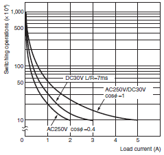
| Control output | Models with Contact Outputs
5 A at 250 VAC/30 VDC, resistive load (cos =1) Minimum applied load: 10 mA at 5 VDC (failure level: P, reference value) Contact materials: AgSnIn Transistor output: NPN open collector, 100 mA at 30 VDC max., residual voltage: 1.5 VDC max. (Approx. 1 V), Leakage current: 0.1 mA max. |
|||
| Display method *3 | 7-segment, negative
transmissive LCD; Present value: 12-mm-high characters, (switchable between red, green, and orange) Set value: 6-mm-high characters, green |
7-segment, negative transmissive LCD;
Present value: 12-mm-high characters, red Set value: 6-mm-high characters, green |
||
| Memory backup | EEPROM (overwrites: 100,000 times min.) that can store data for 10 years min. | |||
| Operating temperature range | -10 to 55°C (-10 to 50°C if counters are mounted side by side) (with no icing or
condensation) |
|||
| Storage temperature range | -25 to 70°C (with no icing or condensation) | |||
| Operating humidity range | 25% to 85% | |||
| Case color | Black (N1.5) (Optional Front Panels are available to change the Front Panel color to
light gray or white.) |
|||
| Attachments | Waterproof packing, flush
mounting adapter, label for DIP switch settings |
Label for DIP switch
settings |
--- | |